
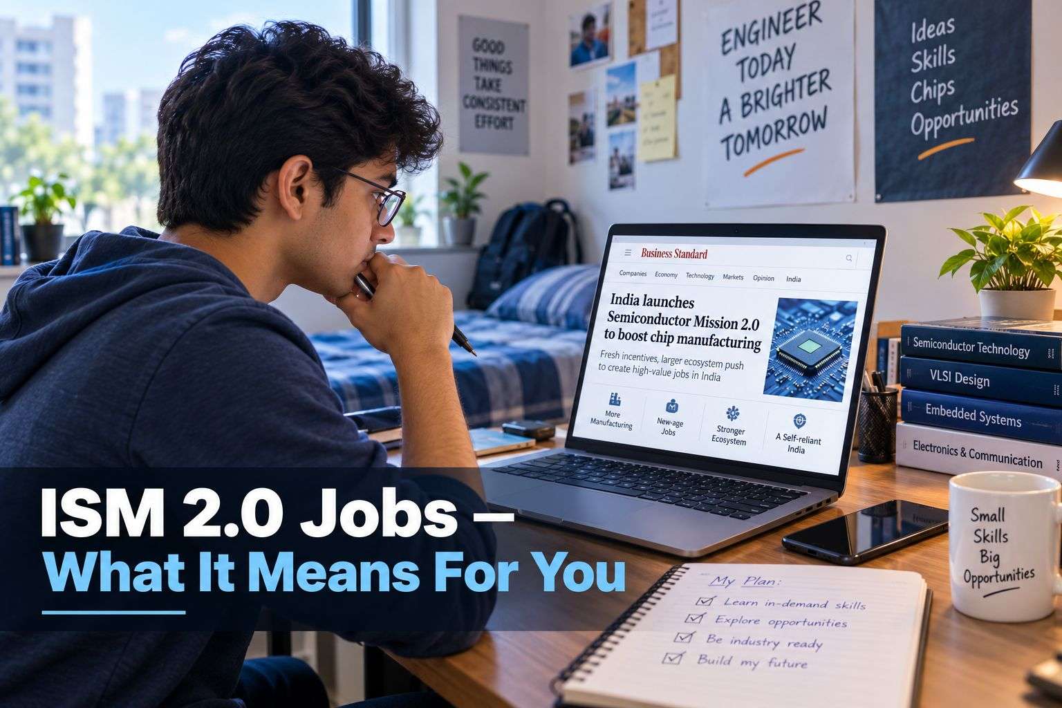
ISM 2.0 Jobs — A 27-Year IT Career Consultant’s Honest Guide to What India’s ₹1.27 Lakh Crore Semiconductor Mission Means for Engineering Students (2026)
ISM 2.0 jobs are the headline every engineering student is scrolling past right now, and I want to stop you before you scroll further. On 4 August 2026, the Union Cabinet approved India Semiconductor Mission 2.0 with an outlay of ₹1.27 lakh crore, and the Ministry of Electronics and IT called 2026 a landmark year for India’s chip industry. Most students read that number, feel a vague sense that something big is happening, and move on to the next reel. I do not want you to do that.
I have spent 27 years counselling engineering students in Bhubaneswar, Cuttack, Rourkela, and Berhampur, and I have watched three or four “this changes everything” waves come and go. Some were hype. This one is not, because ISM 2.0 jobs are backed by cabinet-approved money, real factories already running, and a government skilling push that is already enrolling students. This blog is my honest, no-jargon explanation of what ISM 2.0 jobs actually are, where they are opening, and how you -including a BPUT student in Odisha – can realistically prepare for one.
Table of Contents
- What Is ISM 2.0 — In Plain Language for Students
- Why ISM 2.0 Jobs Are Different From the ISM 1.0 Wave
- ISM 2.0 Jobs – Where the New Roles Are Actually Opening
- The ISM 2.0 Skilling Push — What NIELIT and New Degree Programs Mean for You
- ISM 2.0 Jobs in Odisha — Riding on a Cluster That Already Exists
- What ISM 2.0 Jobs Pay in 2026
- How to Actually Position Yourself for ISM 2.0 Jobs — Year by Year
- Three Mistakes Students Make Chasing ISM 2.0 Jobs
- Watch and Learn More
- FAQs — ISM 2.0 Jobs for Engineering Students in 2026
- What to Do This Week — Your ISM 2.0 Action Plan
What Is ISM 2.0 – In Plain Language for Students
Before anything else, let me explain what ISM 2.0 actually is, because most students have only seen the headline number and nothing else.
ISM stands for India Semiconductor Mission. ISM 1.0 was approved in December 2021 with ₹76,000 crore, and its job was to get India’s first chip factories built at all. ISM 2.0 is the second phase. It was cleared by the Cabinet in August 2026 with an outlay of roughly ₹1.27 lakh crore, and its job is different — it is about going deeper. It focuses on making the equipment and materials that go into chips inside India, building full Indian chip design capability, and training the workforce that all of this needs.
That last part is the part that matters most to you. ISM 2.0 jobs exist because the mission itself has a dedicated skilling component — industry-led research and training centres — written into its design. This is not a side effect of the policy. It is one of its stated pillars.
Why ISM 2.0 Jobs Are Different From the ISM 1.0 Wave
I want to give you three honest reasons why I am telling students to take ISM 2.0 jobs seriously this year, not three years from now.
Reason 1 — the money is already committed, and some of it is already spent. ISM 1.0 has already resulted in twelve manufacturing units approved with over ₹1.64 lakh crore in investment, spanning silicon fabs, a silicon carbide fab, a Gallium Nitride display fab, and nine packaging units. ISM 2.0 builds directly on top of that, not from zero.
Reason 2 — three facilities are already producing chips. As of mid-2026, Micron’s Sanand plant, Tata’s Sanand facility, and CG Power’s unit have all entered commercial production. Two more units are expected to start later this year, and roughly a dozen more are in the pipeline. ISM 2.0 jobs at these sites are not a future promise. They are current job openings.
Reason 3 — the skilling numbers prove the pipeline is real, not theoretical. Over 1 lakh engineers have already been trained and 68,000 people have been skilled specifically in chip design under the government’s semiconductor talent programmes, with 175 chip designs already taped out. That is not a projection in a policy document. That is a number of actual people who have already gone through this pipeline.
I tell my students the same thing about every genuine opportunity. When the money has already been spent and the factories are already running, you are not betting on a promise. You are applying to something real.
ISM 2.0 Jobs — Where the New Roles Are Actually Opening
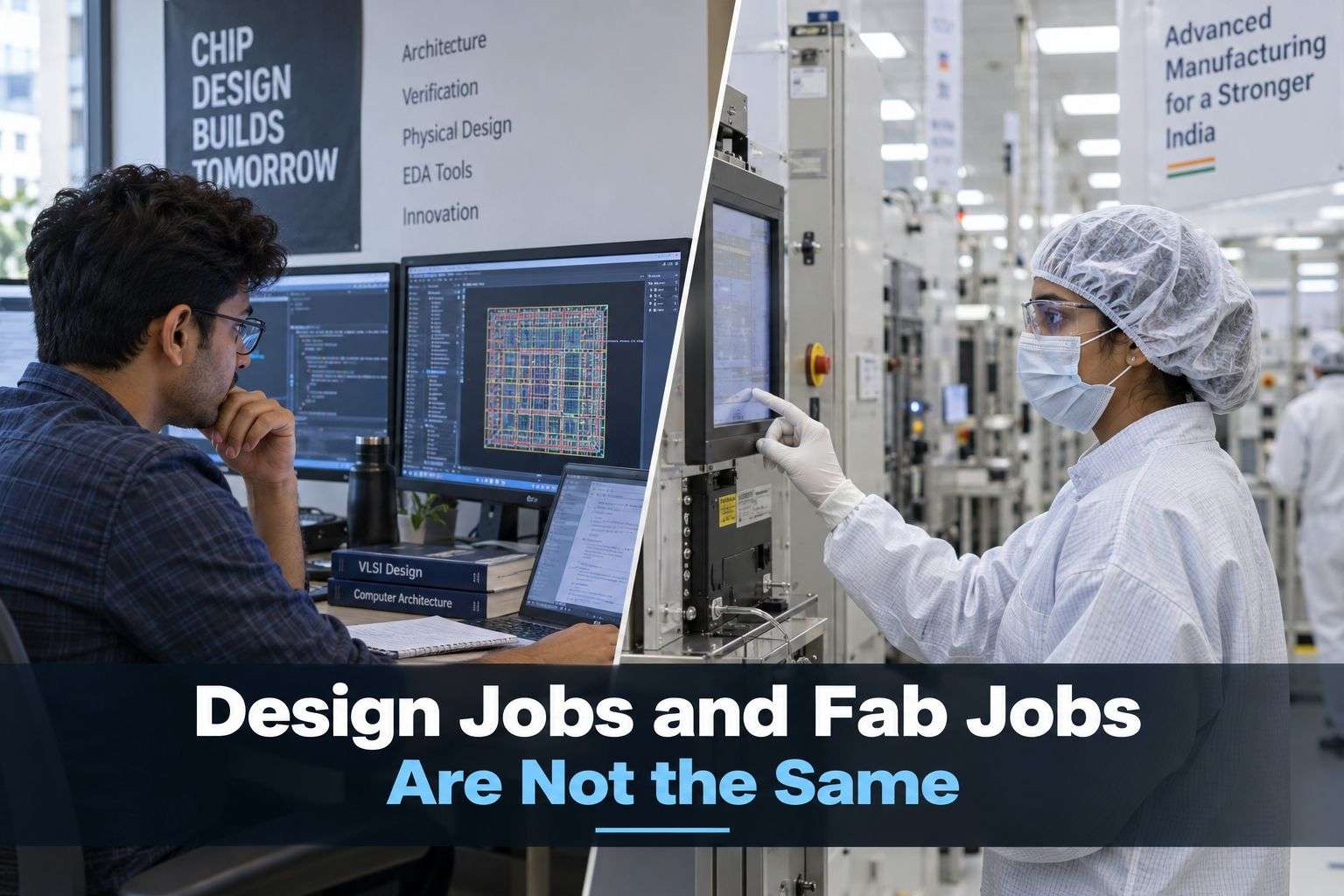
Students often assume ISM 2.0 jobs mean one thing only — chip design. That is only a slice of what this mission is actually creating. Here is where the roles genuinely sit.
Equipment and materials engineering roles are a new category ISM 2.0 specifically targets, since it wants India to manufacture the specialty chemicals, gases, and equipment that fabs need, not just import them. This opens roles for Chemical, Mechanical, and Instrumentation engineers that did not really exist in India two years ago.
Full-stack chip design and IP roles are being expanded through the Design Linked Incentive scheme and the Chips to Startup programme, which gives universities and fabless startups access to expensive design tools they could never otherwise afford.
Fab process and equipment engineering roles continue growing as new facilities under ISM 2.0 come online — the FY27 fab expansion alone is expected to generate around 1,500 high-skilled jobs directly.
ATMP and OSAT roles — assembly, testing, marking, and packaging — are growing even faster in raw numbers. Roughly nine ATMP and OSAT units are expected to attract close to ₹11,000 crore in investment and generate approximately 3,000 jobs.
RISC-V and indigenous processor roles are a newer category under ISM 2.0’s Digital India RISC-V Programme, which promotes open-source processor design without licence costs — a genuinely new avenue for design-focused engineering graduates.
Notice something important here. ISM 2.0 jobs are not concentrated in one role type. They span chemistry, mechanical process work, chip design, and testing — which means your branch does not automatically rule you out, whatever your branch is.
🔗 For a full breakdown of specific semiconductor roles, salaries, and required skills, read our detailed guide: Semiconductor Jobs in India — A Complete Guide for Engineering Graduates
The ISM 2.0 Skilling Push — What NIELIT and New Degree Programs Mean for You
This is the part of the ISM 2.0 story that most students skip past, and I think it is the most actionable section in this entire blog.
The National Institute of Electronics and Information Technology, or NIELIT, is setting up two new Centres of Excellence for semiconductor skilling — one in Ahmedabad and one in Guwahati — specifically to train people in OSAT and ATMP processes. NIELIT has already signed agreements with Tata Electronics and Infineon for these facilities, and is collaborating with other manufacturing plants as well.
NIELIT is also using its Deemed-to-be-University status to launch BTech, MTech, and diploma programs focused specifically on semiconductors and semiconductor manufacturing. This means a structured, government-backed academic route into ISM 2.0 jobs now exists — not just a private certification market of uneven quality.
If your own college has not yet added a semiconductor-focused elective or lab, that does not mean the door is closed. It means you need to look slightly outside your own campus for the training that ISM 2.0 jobs actually reward.
🔗 Related Read: Best Certifications for Freshers in India in 2026
ISM 2.0 Jobs in Odisha — Riding on a Cluster That Already Exists
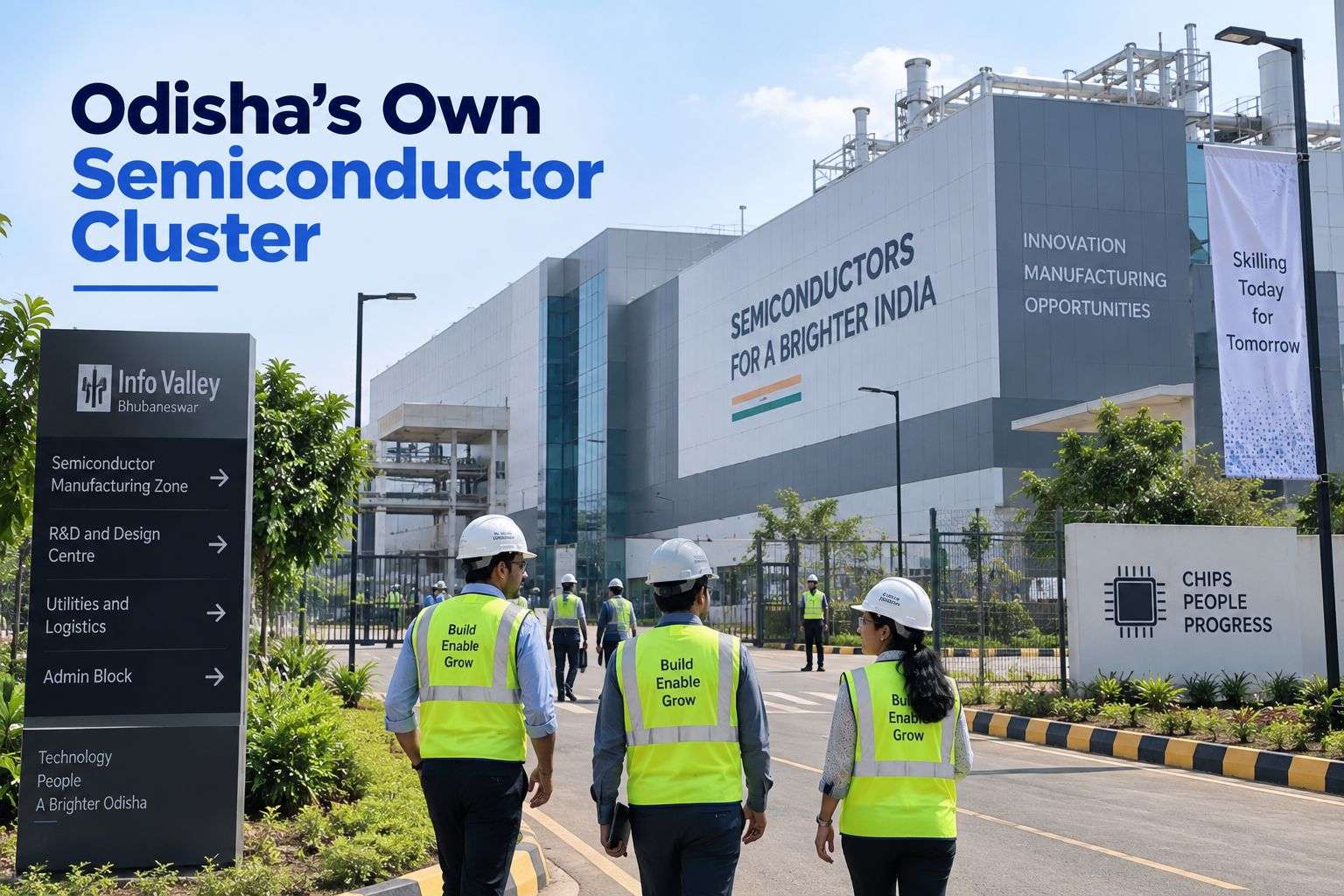
I have written before about SiCSem’s silicon carbide fab coming up at Info Valley in Bhubaneswar, alongside RIR Power Electronics and a 3D Glass Solutions packaging unit backed by Intel. What I want to add here is specific to ISM 2.0.
ISM 2.0’s national skilling push — the NIELIT Centres of Excellence, the new BTech and diploma programs, the industry-led training centres written into the mission — is not limited to Gujarat and Assam. As these skilling frameworks scale nationally, Odisha’s own cluster benefits directly, because the whole point of ISM 2.0 jobs is to build a distributed talent pipeline, not one concentrated only in two or three states.
For a student in Bhubaneswar, Cuttack, or Rourkela, this means two things are happening at once — a local semiconductor cluster that is already hiring, and a national skilling mission that is actively building the training routes you need to qualify for it.
🔗 Related Read: Odisha GCC Policy 2025 — What It Means for Engineering Freshers
What ISM 2.0 Jobs Pay in 2026
I will keep this section honest and brief, because I have already published detailed salary bands by role in my full semiconductor jobs guide, and I do not want to repeat inflated numbers here just to fill space.
Entry-level ATMP, test, and fab process roles under ISM 2.0 jobs typically start between ₹3 and ₹6 LPA at Indian manufacturing units. Fresher VLSI design and verification roles typically start between ₹4 and ₹8 LPA, with meaningfully more at global chip companies with an India presence. Engineers with three to five years of specialised experience in verification, physical design, or fab process work typically move into the ₹9 to ₹14 LPA band.
The honest caveat I give every student — ISM 2.0 jobs reward demonstrated skill, not a degree alone. A fresher with a genuine hands-on project or internship earns meaningfully more than one with a certificate and nothing else to show for it.
🔗 Related Read: Fresher Salary in India 2026
How to Actually Position Yourself for ISM 2.0 Jobs — Year by Year
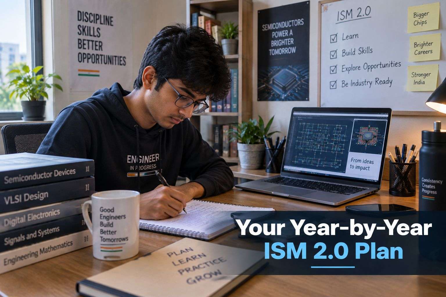
If you are in first or second year — Take your physics, chemistry, and core electronics coursework seriously starting now. ISM 2.0’s equipment and materials push specifically needs students who understand chemistry and materials science deeply, not just electronics. If you are ECE or EEE, start a small Verilog project using free online resources.
If you are in third year — Decide whether design, fab process, or ATMP work interests you more, using the role breakdown earlier in this blog. Look specifically for internship or plant visit opportunities at facilities already in commercial production — Micron, Tata Electronics, CG Power, or here in Odisha, SiCSem and RIR Power Electronics.
If you are in final year — Ask your placement cell directly whether it has approached companies hiring for ISM 2.0 jobs, since this is still a new hiring category most placement cells are catching up on. If your college has not, research the NIELIT Centres of Excellence and any semiconductor-focused diploma or certification programs directly, and apply off-campus if needed.
Structured training programs, including the ones Rooman Technologies runs across Odisha, are also beginning to add semiconductor and electronics manufacturing tracks — worth checking if your own college does not yet have direct industry access.
Three Mistakes Students Make Chasing ISM 2.0 Jobs
Mistake 1 — treating ISM 2.0 as just a budget headline. Students read the ₹1.27 lakh crore number, feel impressed, and do nothing with it. The actual actionable information — NIELIT’s new Centres of Excellence, the specific job numbers by category — is buried under the policy language. Read past the headline.
Mistake 2 — assuming every ISM 2.0 job needs an ECE degree. Equipment, materials, and fab process roles under ISM 2.0 genuinely suit Mechanical, Chemical, and Instrumentation graduates. Do not rule yourself out before checking the actual requirements.
Mistake 3 — waiting for a formal college course before starting. NIELIT’s new BTech and diploma programs are still scaling up. Students who start building fundamentals now, using free resources and internships, will be ahead of classmates who wait for a formal course to appear on their own campus.
🔗 Related Read: Campus Placements 2026 Are Back — The 82,000 Fresher Hiring Surge 🔗 Related Read: Top Tech Skills Employers Look for in Freshers in India 2026
Watch and Learn More
🎥 India Semiconductor Mission 2.0 Explained — Budget 2026 and India’s Chip Revolution 🎥 ISM 2.0: From Chip Fabs to a Full-Stack Ecosystem 🎥 In-Depth: India Semiconductor Mission 2.0
FAQs — ISM 2.0 Jobs for Engineering Students in 2026
FAQ 1 — What exactly is the difference between ISM 1.0 and ISM 2.0, and why does that difference matter for job seekers?
ISM 1.0, approved in December 2021 with ₹76,000 crore, was mainly about getting India’s first fabs and packaging units built at all. It succeeded in that narrow goal — twelve manufacturing units are now approved with over ₹1.64 lakh crore in investment. ISM 2.0, approved in August 2026 with roughly ₹1.27 lakh crore, is about going deeper — building the equipment and materials supply chain inside India, developing full Indian chip design IP, and formally embedding skilling and training centres into the mission itself.
For a job seeker, this difference matters because ISM 1.0 jobs were concentrated almost entirely in the handful of states where the first fabs came up. ISM 2.0 jobs are structured to be more distributed, because the mission’s own skilling component is explicitly designed to build a national talent pipeline, not a regional one.
Consultant’s Note — I tell students that policy phases matter more than they realise. ISM 1.0 was about proving the concept. ISM 2.0 is about scaling it and training people for it. If you are entering the job market now, you are entering at the scaling stage, which is usually the stage with the most actual hiring volume.
FAQ 2 — Are ISM 2.0 jobs only in chip design, or is there real opportunity in the manufacturing and equipment side too?
This is one of the most common assumptions I have to correct. ISM 2.0 specifically targets equipment and materials manufacturing as one of its core pillars — producing the specialty chemicals, gases, and machinery that fabs need, rather than importing all of it. That is a genuinely new job category with real openings for Mechanical, Chemical, and Instrumentation engineers, separate from chip design entirely.
The mission’s manufacturing focus also includes direct fab expansion, expected to create around 1,500 high-skilled jobs in FY27 alone, plus ATMP and OSAT expansion expected to add roughly 3,000 more. Chip design gets more attention in the media, but manufacturing-side ISM 2.0 jobs are opening in larger numbers right now.
Consultant’s Note — I have watched students dismiss ISM 2.0 jobs because they assumed it all meant coding chip logic. Once they see the equipment, materials, and ATMP numbers, several realise their own branch fits better than they expected. Read the actual role categories before deciding this mission is not for you.
FAQ 3 — How can a student verify that ISM 2.0 job openings are real and not just policy language with no actual hiring behind it?
This is a fair and important question, because policy announcements do not always translate into hiring immediately. The honest answer is that ISM 2.0 sits on top of an ISM 1.0 foundation that has already converted into real jobs — three facilities, including Micron, Tata’s Sanand plant, and CG Power, are already in commercial production, and two more are expected to start operations later this year.
Separately, the skilling side of this mission has already produced measurable results — over 1 lakh engineers trained and 68,000 people skilled specifically in chip design, with 175 chip designs already taped out. These are not projections. These are counts of people who have already gone through this pipeline and, in many cases, into roles.
Consultant’s Note — I tell students to always check whether a policy has a “before and after” number, not just a “will do” promise. ISM 2.0 has both -approved investment figures and already-trained-people figures. That combination is what makes me comfortable telling students to take this seriously.
FAQ 4 — What is the realistic timeline for a fresher with no prior semiconductor exposure to actually land one of these ISM 2.0 jobs?
The timeline depends heavily on which category of role you target. For ATMP, test, or fab process roles at facilities already in commercial production, a fresher with strong fundamentals and even a short internship or plant visit on their resume can realistically expect to clear interviews within three to six months of active searching, given how quickly these facilities are ramping up hiring.
For chip design and verification-focused ISM 2.0 jobs, the timeline is usually longer — six months to a year — because these roles are more competitive and typically require a demonstrable project, not just a certificate. The single biggest variable, in either case, is whether you have done anything hands-on beyond classroom coursework.
Consultant’s Note — I tell every student the same thing about any emerging job category. The timeline shortens the moment you have something concrete to show. Marks alone open far fewer doors than they used to, and that is especially true for a new category like this one.
FAQ 5 — Do the new NIELIT semiconductor Centres of Excellence accept students from outside Ahmedabad and Guwahati, or is this limited to local colleges?
NIELIT’s Centres of Excellence are being physically located in Ahmedabad and Guwahati, but NIELIT operates as a Deemed-to-be-University with a national mandate, and its new BTech, MTech, and diploma programs focused on semiconductors are part of a broader national skilling framework, not a purely local one.
Students outside these two cities should specifically check NIELIT’s admission and outreach programs rather than assuming the opportunity is geographically closed to them. Given that ISM 2.0’s entire purpose is building a distributed national talent pipeline, it would work against the mission’s own goals to restrict this purely to two cities.
Consultant’s Note — I tell students not to assume a national skilling institute’s physical address is the same as its actual reach. Always check the admission process directly before ruling yourself out based on geography alone.
FAQ 6 — Should a Mechanical or Chemical engineering student specifically target ISM 2.0’s equipment and materials push, or is this really meant for core process engineers only?
ISM 2.0’s equipment and materials pillar is precisely the part of this mission built for Mechanical, Chemical, and Instrumentation graduates. Producing the specialty chemicals, gases, and precision equipment that fabs require draws directly on materials science, chemical processing, and mechanical precision engineering — subjects these students study in depth, sometimes more deeply than ECE students do.
This is a genuinely underexplored angle among students right now, because most conversations around semiconductor careers default to chip design. A Mechanical or Chemical engineering student who takes the time to understand this pillar specifically stands out, precisely because fewer of their classmates are looking at it.
Consultant’s Note — I have counselled several Mechanical students who assumed the entire semiconductor story was closed to them. ISM 2.0’s equipment and materials focus is the clearest evidence yet that it is not. Check this pillar specifically before you default to a purely IT career path.
FAQ 7 — How does the Design Linked Incentive scheme and the Chips to Startup programme under ISM 2.0 create job opportunities for students, not just companies?
The Design Linked Incentive scheme provides financial support to fabless chip design companies and startups, which directly translates into more hiring at these companies as they scale their design teams. The Chips to Startup programme gives universities and startups access to expensive Electronic Design Automation tools that they could never otherwise afford, which means students at participating institutions get hands-on exposure to industry-grade design tools before they even graduate.
For a student, this combination matters because it lowers the barrier to building a genuine, demonstrable chip design project during college — the exact kind of project that shortens your path into ISM 2.0 jobs after graduation.
Consultant’s Note — I tell students to check whether their own college or a nearby institution has access to these EDA tools through the Chips to Startup programme. If it does, that access is worth more to your resume than most paid certifications you would otherwise consider.
FAQ 8 — Is there a risk that ISM 2.0 jobs will be automated away by AI before students entering college now can benefit from them?
This is a fair concern for any emerging field in 2026. AI tools are already used inside chip design workflows for layout optimisation and defect detection in manufacturing. What this changes is the nature of the work, not the underlying need for people.
Physical manufacturing and equipment roles under ISM 2.0 have a natural limit to how much AI can replace, because someone still needs to physically operate, calibrate, and troubleshoot equipment inside a fab. Design and verification roles increasingly involve reviewing AI-assisted outputs rather than manual work from scratch, which raises the skill bar rather than removing the role entirely.
Consultant’s Note — I tell students the same thing about AI and every emerging career. AI is changing what “understanding your work” means, not removing the need for people who understand it deeply. A student who builds genuine fundamentals now will work productively alongside these tools later.
FAQ 9 — What should a first-year engineering student in a tier-2 Odisha college actually do this month if ISM 2.0 jobs are their goal three or four years from now?
Start with your fundamentals, not with a certification purchase. If you are ECE or EEE, spend this month completing the first module of a free Verilog tutorial and read about basic CMOS concepts beyond what your syllabus strictly requires. If you are Mechanical, Chemical, or Instrumentation, spend time understanding what a cleanroom actually is and how semiconductor materials processing differs from general manufacturing.
Separately, follow ISM 2.0 news specifically — not general tech news — so you notice new skilling programs, NIELIT admissions, or company hiring announcements as they happen, rather than hearing about them a year late from a classmate.
Consultant’s Note — I tell first-year students the same thing regardless of which emerging field they are eyeing. The subjects your syllabus already makes you study are rarely wasted time. For ISM 2.0 jobs specifically, your basic physics, chemistry, and electronics fundamentals are the actual job, not background noise before the real work starts.
FAQ 10 — How does a student decide between preparing for ISM 2.0 jobs versus a more established IT career path?
This is ultimately a personal decision, and I want to give you an honest framework rather than push you toward either path. IT and software careers in India remain more established, with a larger volume of open roles and a more mature, predictable hiring process — but also correspondingly higher competition, since far more students are actively preparing for them.
ISM 2.0 jobs are earlier in their growth curve, with fewer total open roles right now compared to IT, but meaningfully less competition per role, backed by cabinet-approved funding and a national skilling mission actively building the training pipeline for you. If you have a genuine interest in physical engineering, chemistry, materials, or hardware — not just a general interest in finding any good job — this earlier stage works in your favour.
Consultant’s Note — I never tell a student to chase a field purely because a headline number sounds large. I ask what they actually enjoyed in their coursework first. Students who do best in ISM 2.0 jobs are consistently the ones already drawn to electronics, chemistry, or physical systems, not the ones chasing a trend after reading one budget headline.
What to Do This Week — Your ISM 2.0 Action Plan

If you are in first or second year — Pick one ISM 2.0 pillar that matches your branch — design for ECE and EEE, equipment and materials for Mechanical and Chemical — and spend thirty minutes this week reading about what that pillar actually involves, beyond the budget headline.
If you are in third year – Research NIELIT’s Centres of Excellence and any semiconductor-focused BTech, MTech, or diploma programs directly. Even if you cannot enrol immediately, understanding the admission process now saves you months later.
If you are in final year — Ask your placement cell directly whether companies connected to ISM 2.0’s fab, ATMP, or design expansion have been approached for campus drives. If not, research off-campus openings at facilities already in commercial production, including the ones ramping up hiring in Odisha right now.
ISM 2.0 jobs are at the exact stage every genuinely good opportunity passes through once — the stage where the funding is real, the factories are running, and most students have still not connected the two. I have watched this exact window happen with cloud computing, with AI roles, and with general semiconductor jobs. The students who read past the budget headline this month are the ones who will be building a genuine ISM 2.0 career while their classmates are still debating whether it is real.
Start with the pillar that matches your branch. That is where every ISM 2.0 career actually begins.
Completing your career research? Read our guides on Semiconductor Jobs in India — A Complete Guide for Engineering Graduates and Odisha GCC Policy 2025 to understand how India’s evolving job market fits into your broader engineering career plan.
Sources referenced: