
Semiconductor Jobs in India — A 27-Year IT Career Consultant’s Honest Guide for Engineering Graduates in 2026
Semiconductor jobs in India are not a future promise anymore. They are showing up in offer letters right now, in 2026, and most engineering students I counsel have still not connected the dots.
Here is the number that should make you sit up. As of May 2026, the central government has approved 13 semiconductor projects across seven states—fabs, packaging units, and testing facilities — with cumulative investment crossing ₹1.64 lakh crore. That is not a policy announcement sitting in a file somewhere. Tata’s Dholera fab is targeting first silicon by the end of this year. Micron’s plant in Sanand is already running. And closer home, a compound semiconductor fab is coming up in Bhubaneswar, right here in Odisha.
I have spent 27 years telling students to be careful about hype. IT has seen many “next big thing” waves come and go. But semiconductor jobs in India are different from most of those waves, because this one is backed by physical factories, government money already spent, and a genuine domestic skill shortage. This blog is my honest, no-hype explanation of what these jobs actually are, what they pay, and how an engineering graduate — including one from Odisha — can realistically get into this field.
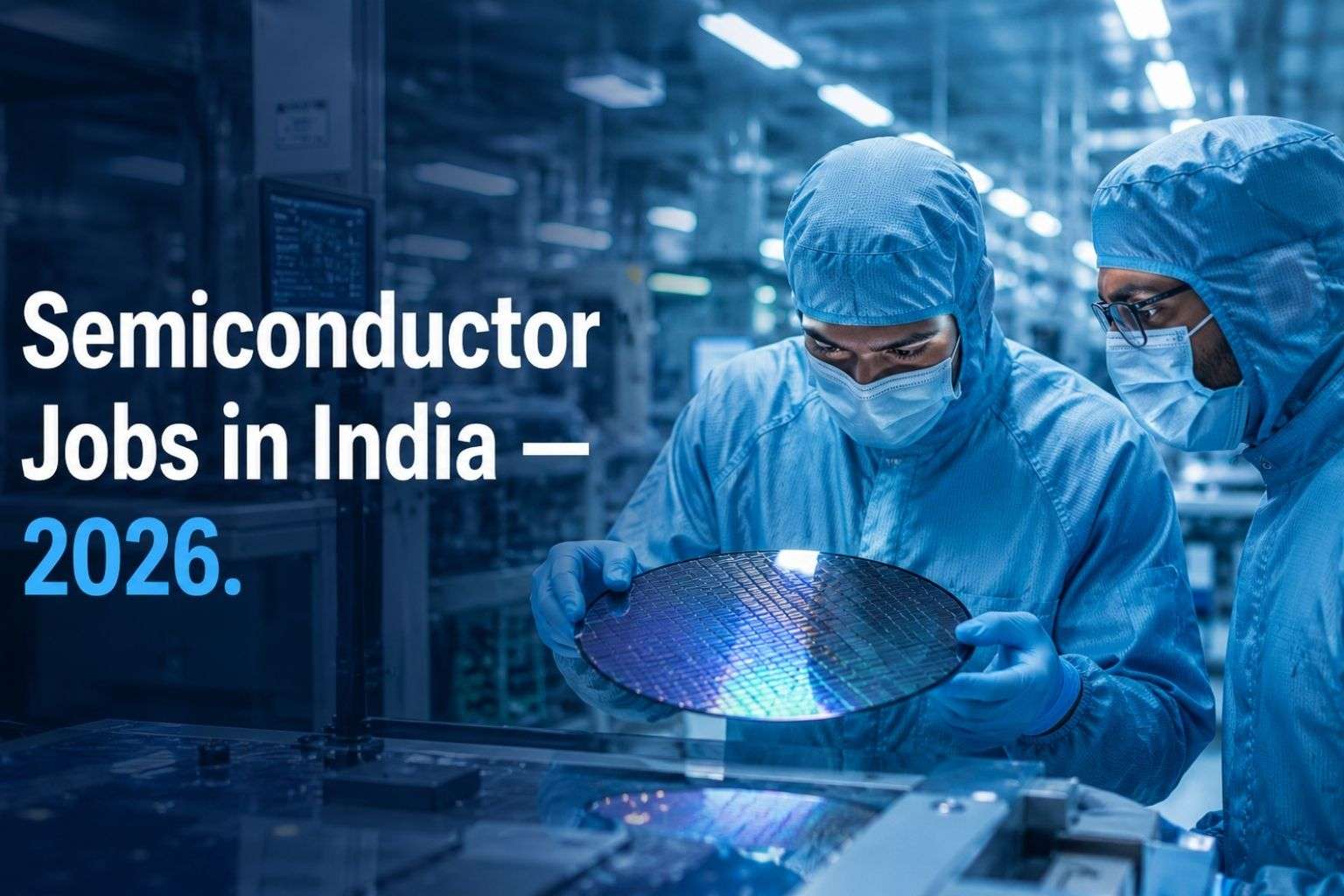
What Are Semiconductor Jobs — In Plain Language
Before anything else, let me explain what this industry actually does, because most students have a vague idea built from news headlines and nothing more.
A semiconductor is the chip inside every phone, laptop, car, and appliance you own. Someone has to design that chip. Someone has to manufacture it in a factory called a fab. Someone has to test it, package it, and make sure it works before it ships. Semiconductor jobs in India cover all three of these stages — design, fabrication, and packaging — and each stage needs a different kind of engineer.
Design work happens mostly in Bengaluru, Hyderabad, and Chennai, where global chip companies already run large design centres. This is where you write the logic that becomes a chip, using languages like Verilog and tools from companies like Cadence and Synopsys.
Fabrication and packaging are newer to India. This is the physical manufacturing — growing silicon wafers, etching circuits onto them, testing each chip, and packaging it for shipment. These jobs are opening in Gujarat, Assam, and now Odisha, as the new fabs come online through 2026 and 2027.
Both halves of this industry need engineers. And both halves are hiring right now.
Why Semiconductor Jobs in India Are a Genuine New Career Path — Not Hype
I want to give you three honest reasons why I am telling students to take this seriously in 2026, not three years from now.
Reason 1 — the money has already been spent. India’s Semiconductor Mission has committed roughly ₹76,000 crore in direct fiscal support, and state governments have layered their own incentives on top of that. This is not a plan on paper. Tata’s fab in Dholera, Micron’s facility in Sanand, and Kaynes Semicon’s packaging unit are physically built and running or close to it.
Reason 2 — the talent pipeline does not exist yet. India already has roughly a fifth of the world’s chip design engineers, but almost none of them have manufacturing experience, because India never had commercial fabs before now. That gap is exactly where a fresh engineering graduate willing to learn fits in.
Reason 3 — it is not concentrated in the usual four cities anymore. Semiconductor jobs in India used to mean Bengaluru, full stop. That is changing. Gujarat, Assam, and Odisha now have real semiconductor investment, which means students from tier-2 states are no longer applying from the outside looking in.
Semiconductor Jobs in India — The Roles You Can Actually Target
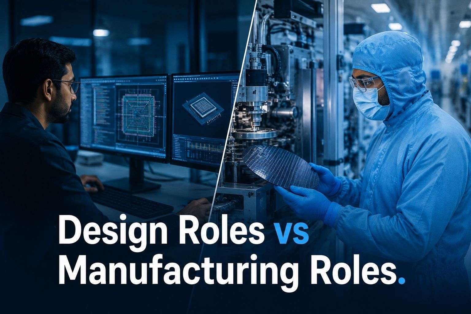
Students often assume semiconductor careers mean one thing — chip design. That is only one slice of a much bigger picture. Here are the roles that are genuinely hiring engineering graduates in 2026.
VLSI Design Engineer — writes the hardware logic for a chip using Verilog or SystemVerilog. This is the most competitive and most talked-about role, concentrated in Bengaluru, Hyderabad, and Chennai.
Verification Engineer — builds test environments to prove a chip design actually works before it goes to manufacturing. High demand, and a strong entry point for ECE graduates with good fundamentals.
Physical Design Engineer — takes a verified chip design and works out floorplanning, placement, and timing so it can actually be manufactured.
Fab Process Engineer — works inside the fab itself, on lithography, etching, and deposition — the physical steps that turn a silicon wafer into a working chip. This role barely existed in India two years ago. It exists now.
Test and ATMP Engineer — works in assembly, testing, marking, and packaging facilities, checking that finished chips actually work before they ship. This is one of the fastest-growing categories of semiconductor jobs in India right now, because every new fab needs this stage.
Equipment and Quality Engineer — maintains and calibrates the specialised machinery inside a fab, and manages quality and reliability standards. Mechanical and instrumentation engineers fit naturally here.
Notice something important. Not every one of these roles needs a VLSI background. Fab process, equipment, and quality roles are open to Mechanical, Electrical, Instrumentation, and even Chemical engineering graduates — not just ECE.
Semiconductor Jobs in Odisha — What Is Actually Happening in Bhubaneswar

This is the part of the semiconductor story that most students in Odisha do not know yet, and I think it is the most important section of this entire blog for my readers in Bhubaneswar, Cuttack, and Rourkela.
SiCSem Private Limited, a subsidiary of Archean Chemical Industries, is building India’s first commercial compound semiconductor fab — a silicon carbide facility — at Info Valley in Bhubaneswar. This is not a small pilot project. It is expected to process 60,000 wafers a year with a packaging capacity of 96 million units, and it is projected to create around 5,000 direct and indirect jobs in the region.
Alongside SiCSem, RIR Power Electronics is setting up its own silicon carbide wafer fabrication plant in the same Info Valley cluster, and 3D Glass Solutions is building an advanced packaging unit backed by Intel — all within Odisha’s Electronics Component Manufacturing Policy 2025, which offers capital subsidies and training support for large projects.
Read that again. This is not a “someday” story for Odisha students. It is happening in Khordha district, an hour from most BPUT-affiliated colleges. Silicon carbide chips like these go into electric vehicles, defence equipment, solar inverters, and fast chargers — some of the fastest-growing electronics categories in the country.
If you are studying Electronics, Electrical, Instrumentation, or even Mechanical engineering in Odisha, this is a semiconductor job market opening up in your own state, not one you need to relocate for on day one.
What Semiconductor Jobs in India Pay in 2026
Let me give you honest numbers, not inflated ones.
Fresher — Fab, Test, or ATMP Engineer. Entry-level roles typically start between ₹3 and ₹6 LPA at Indian manufacturing units, with strong performers moving up faster than in most traditional core-engineering jobs.
Fresher — VLSI Design or Verification Engineer. Freshers with genuine project experience and strong fundamentals can expect ₹4 to ₹8 LPA at Indian design centres, and considerably more at global chip companies with an India presence.
Mid-Level — 3 to 5 Years Experience. Semiconductor engineers with specialised skills in verification, physical design, or fab process engineering typically earn between ₹9 and ₹14 LPA, with top performers crossing ₹20 LPA.
Senior and Specialist Roles. Experienced design and process engineers at global chipmakers can earn ₹25 to ₹35 LPA and beyond, depending on the specialisation and company.
The honest caveat I give every student — semiconductor salaries reward depth, not just a degree. A fresher with a genuine VLSI or fab project on their resume earns meaningfully more than one with a certificate alone. This is true across every core-engineering field, not just semiconductors.
🔗 Related Read: Fresher Salary in India 2026
Skills You Actually Need for Semiconductor Jobs in India

Students ask me this constantly, so let me be specific rather than generic.
For design and verification roles, you need strong fundamentals in digital electronics, CMOS basics, and hands-on comfort with Verilog or SystemVerilog. Familiarity with EDA tools like Cadence or Synopsys is a genuine advantage, even at a basic level from a college lab or online course.
For fab and process roles, the fundamentals shift. You need strong basics in materials science, chemistry, and physics — lithography, etching, and deposition are chemistry-and-physics-heavy processes, not coding-heavy ones. Mechanical and Instrumentation students often have a natural head start here.
For test and ATMP roles, scripting comfort in Python helps, along with genuine attention to detail — these roles involve checking thousands of chips for defects, and small errors are expensive.
For every role, employers increasingly expect basic familiarity with data analysis, since fabs generate enormous amounts of process data that engineers are expected to read and act on.
None of this requires an M.Tech to start. A B.Tech graduate with strong fundamentals, one or two genuine hands-on projects, and a willingness to relocate for the first two to three years has a real shot at semiconductor jobs in India in 2026.
🔗 Related Read: Top Tech Skills Employers Look for in Freshers in India 2026
How to Actually Get Into Semiconductor Jobs in India — Year by Year
If you are in first or second year — Strengthen your core electronics, physics, and chemistry fundamentals now. Do not treat these as “just theory subjects” to clear exams. They are the actual foundation of semiconductor work. Start a small Verilog project if you are ECE, or read up on materials science and clean-room basics if you are Mechanical or Instrumentation.
If you are in third year — Pick a lane. If chip design interests you, build a genuine RTL design or verification mini-project, even a simple one, and put it on GitHub with proper documentation. If fab or process engineering interests you more, look for a summer internship at any of the operational facilities — Micron, Tata Electronics, CG Power, or here in Odisha, SiCSem or RIR Power Electronics — even a short exposure visit builds real understanding.
If you are in final year — Target campus drives specifically from semiconductor and electronics manufacturing companies, not only the usual IT services firms. Many of these companies are actively recruiting from BPUT-affiliated colleges as the Odisha facilities ramp up hiring. If your college has a placement cell, ask directly whether semiconductor or electronics manufacturing companies have been approached — this is a new category most placement cells are still catching up on.
Structured training programs, including the ones Rooman Technologies runs across Odisha, are also starting to add semiconductor and electronics manufacturing tracks alongside the traditional IT ones — worth checking if your college does not have direct industry access yet.
Three Mistakes Students Make Chasing Semiconductor Jobs in India
Mistake 1 — assuming it is only for ECE toppers. Fab, test, and ATMP roles are genuinely open to Mechanical, Electrical, and Instrumentation graduates. Do not rule yourself out before checking the actual job description.
Mistake 2 — ignoring the manufacturing side because design sounds more prestigious. Design roles are more competitive precisely because every student chases them. Manufacturing and testing roles are hiring in far larger numbers right now, with less competition.
Mistake 3 — waiting for the industry to “mature” before preparing. By the time an industry looks mature and safe, the easy entry window has usually closed. Students who build fundamentals now, while these fabs are still ramping up hiring, have a real head start over those who wait two more years.
🔗 Related Read: Odisha GCC Policy 2025 — What It Means for Engineering Freshers 🔗 Related Read: Best Certifications for Freshers in India in 2026 🔗 Related Read: Cloud Developer vs Cloud Engineer Career in India
Watch and Learn More
🎥 Semiconductor and VLSI Careers in India 2026 — Skills, Scope, Myths Explained by ChipEdge CEO 🎥 Future of VLSI — Top Semiconductor Jobs in India for 2026 🎥 VLSI Roadmap 2026 — Semiconductor Jobs Coming to India
FAQs — Semiconductor Jobs in India 2026
FAQ 1—Can a student from a non-ECE branch—mechanical, Electrical, or instrumentation—realistically get semiconductor jobs in India, or is this field only for electronics graduates?
This is one of the most common questions I get, and I want to be direct about it. Chip design roles—VLSI, verification, physical design—genuinely favour ECE and EEE graduates because the fundamentals required are specific to those degrees. But that is only one part of the semiconductor industry.
Fab process engineering, equipment engineering, and quality engineering roles are built around materials science, chemistry, physics, and precision instrumentation — subjects that Mechanical, Instrumentation, and Chemical engineering students study just as deeply, sometimes more so. Companies setting up new fabs in India, including the one coming up in Bhubaneswar, need engineers across all these disciplines, not only electronics graduates.
What matters more than your branch is whether you can demonstrate genuine understanding of the specific process your target role involves. A Mechanical engineer who has taken the time to understand cleanroom protocols, semiconductor materials, and precision manufacturing stands a real chance at fab and equipment roles.
Consultant’s Note — I have counselled Mechanical and Instrumentation students who assumed semiconductor careers were closed to them simply because they were not from ECE. Once they understood that fab and equipment roles are a completely different skill set from chip design, several of them actively pursued this path with genuine confidence. Do not rule yourself out based on your branch name alone. Check the actual role requirements first.
FAQ 2 — How is a semiconductor job in India different from a regular core engineering job, and does it pay better?
Students often lump semiconductor roles into the general “core engineering” bucket, but the two are meaningfully different in both nature and pay.
Traditional core engineering jobs in India—in sectors like general manufacturing, construction, or heavy engineering—have historically offered lower starting salaries than IT roles, which is exactly why so many engineering graduates have moved toward software careers over the last two decades.
Semiconductor manufacturing breaks that pattern. Because it combines advanced manufacturing with a genuine national skill shortage and heavy government investment, starting salaries and growth trajectories in semiconductor roles are closer to IT sector pay scales than to traditional core engineering pay scales.
The work itself is also different. Semiconductor manufacturing involves working with extremely precise tolerances, cleanroom environments, and specialised equipment that most traditional core engineering roles do not involve. It sits at the intersection of core engineering discipline and advanced technology—which is exactly why I tell students it deserves serious consideration even if they had written off “core jobs” as lower-paying by default.
Consultant’s Note — I have seen students choose IT over core engineering purely because of the salary gap, without knowing that semiconductor manufacturing pays meaningfully closer to IT scales while using their actual engineering fundamentals. If you enjoyed your core subjects and were only avoiding core jobs because of pay, semiconductor manufacturing deserves a proper look before you default to IT.
FAQ 3 — What is the realistic timeline from graduation to landing a semiconductor job in India for a fresher with no prior industry exposure?
This depends heavily on which category of role you are targeting, and I want to give you an honest range rather than a single optimistic number.
For fab, test, or ATMP roles at operational facilities, a fresher with strong fundamentals and a genuine internship or plant visit on their resume can realistically expect to clear interviews and receive an offer within three to six months of active searching, particularly given how quickly new facilities are ramping up hiring in 2026.
For chip design and verification roles, the timeline is typically longer — six months to a year — because these roles are more competitive and usually require a demonstrable project, not just certification. Students who begin building a genuine RTL or verification project in their third year, rather than starting from zero in final year, cut this timeline down significantly.
The biggest variable in either case is not talent—it is whether the student has done anything hands-on beyond classroom coursework. A resume with only academic marks and no project or internship exposure takes noticeably longer to convert into interviews, regardless of which category of role you are targeting.
Consultant’s Note — I tell every student the same thing about semiconductor careers that I tell them about IT careers. The timeline shortens dramatically the moment you have something concrete to show—a project, an internship, a plant visit report. Marks alone open far fewer doors than they used to.
FAQ 4 — Do semiconductor companies in India actually hire freshers directly from tier-2 colleges in Odisha, or only from IITs and NITs?
This is a fair concern, because for years, core engineering hiring in India has skewed heavily toward top-tier institutes for the most competitive roles. But the picture for semiconductor jobs in India in 2026 is more open than that pattern suggests, particularly for manufacturing-side roles.
Design roles at global chip companies in Bengaluru and Hyderabad do skew toward strong academic pedigree, including IITs and NITs, especially for the most competitive positions. But fab, test, ATMP, and equipment roles at the new manufacturing facilities — including the ones coming up in Odisha — are being staffed at much larger volume, and companies setting up fresh operations in a new state genuinely need to hire locally to build a stable, long-term workforce.
For a BPUT-affiliated student in Odisha specifically, the Bhubaneswar semiconductor cluster is a real, local opportunity that does not require competing against IIT graduates for the same seats, because these are largely different role categories with different hiring pools.
Consultant’s Note — I always tell my Odisha students the same thing about new industries arriving in the state. Being early and local is an advantage, not a disadvantage. Companies setting up their first Odisha workforce are not filtering purely on college pedigree the way an established Bengaluru design centre might. Show up prepared, and your BPUT degree is not the barrier you might assume it is.
FAQ 5—What is the difference between working at a chip design company versus working at a fab or ATMP facility, in terms of day-to-day work and career growth?
This distinction matters more than most students realise when they are choosing which path to prepare for.
Chip design work is largely desk-based—writing code, running simulations, debugging designs on a computer, often in a standard office environment. Career growth in design follows a fairly familiar IT-style trajectory — you move from junior engineer to senior engineer to lead, gaining seniority mostly through technical depth and project ownership.
Fab and ATMP work is hands-on and shift-based. You are physically present in a cleanroom or manufacturing floor, working with equipment, monitoring processes, and troubleshooting issues as they happen in real time. Shifts often include night rotations, since fabs run continuously. Career growth here follows more of a traditional manufacturing trajectory — from process engineer to senior process engineer to shift lead to plant-level roles — with genuine long-term stability, since a physical fab does not relocate the way an IT project can.
Neither path is objectively better. It depends on whether you prefer desk-based technical depth or hands-on physical process work, and whether shift-based schedules are something you are comfortable planning your life around.
Consultant’s Note — I ask every student this directly before they commit to a path. Do you like sitting with a problem at a screen for hours, or do you like being on your feet, physically troubleshooting something in front of you? Both are valid engineering careers.
Choose based on how you actually like to work, not based on which sounds more prestigious on LinkedIn.
FAQ 6 — What certifications or additional courses genuinely help for semiconductor jobs in India, and which ones are a waste of money?
Students ask me this because the certification market around every emerging industry, including semiconductors, fills up quickly with courses of wildly varying quality.
For design and verification roles, short, focused courses covering Verilog, SystemVerilog, and basic EDA tool usage — offered by recognised VLSI training institutes — genuinely help, provided they include hands-on lab work, not just video lectures. A certificate that only covers theory without any tool-based practice adds very little to your resume.
For fab and process roles, formal semiconductor manufacturing certifications are less standardised in India right now, since the industry itself is still young here. What helps more concretely is any structured exposure to cleanroom protocols, materials science fundamentals, or a genuine plant visit or internship — even a short one — because interviewers in this space are testing for practical understanding, not certificate names.
What I actively warn students against is paying large sums for generic “semiconductor career” courses that promise placement without any hands-on lab or project component. If a course cannot show you what tools or processes you will actually touch, be skeptical before paying.
Consultant’s Note — I tell students the same thing here that I tell them about every emerging field. The certificate is never the point. What you can actually do with your hands, whether that is writing working Verilog code or explaining a wafer fabrication step correctly, is what gets you through a real interview. Spend your money on hands-on exposure, not on certificate collection.
FAQ 7 — Is a semiconductor career in India safe from AI-driven automation, or should students worry about this the way they worry about IT jobs?
Students are right to ask this about any career path in 2026, and semiconductors are no exception.
AI tools are already being used inside chip design workflows—for layout optimisation, verification test generation, and defect detection in manufacturing.
What this changes is the nature of the work, not the need for people. A verification engineer today is expected to review and validate AI-assisted test results rather than write every test case manually. A fab engineer increasingly works alongside AI-based defect detection systems rather than relying purely on manual inspection.
Physical manufacturing has a natural limit to how much AI can replace, because someone still needs to physically operate, calibrate, and troubleshoot the equipment inside a fab – a fundamentally physical constraint that pure software roles do not have. This is actually one reason I tell students that fab and ATMP roles carry a genuine long-term stability that some software-only careers do not.
Consultant’s Note – I tell every student the same thing about AI and semiconductor careers that I tell them about AI and every other field. AI is raising the bar for what “understanding your work” means, not removing the need for people who understand it. A fab engineer or verification engineer who genuinely understands the underlying process will work alongside these AI tools productively. Someone who only knows surface-level steps will struggle more, not because of AI directly, but because they never had a deep understanding to begin with.
FAQ 8 — Should a student in Odisha specifically target the Bhubaneswar semiconductor cluster, or is it better to move to Gujarat or the south for a semiconductor career?
This is a genuinely practical question I get from students weighing local opportunity against established hubs, and my honest answer depends on your specific goal.
If your priority is chip design specifically, Bengaluru, Hyderabad, and Chennai remain the established centres with the deepest concentration of design companies, and relocating there gives you access to the widest range of design opportunities. Gujarat, particularly Sanand and Dholera, is now the strongest hub for large-scale fab and ATMP roles, given the scale of Tata’s and Micron’s operations there.
For a student specifically interested in fab, test, or ATMP roles who also wants to stay close to home, the Bhubaneswar cluster – SiCSem, RIR Power Electronics, and the 3D Glass Solutions packaging unit— is a genuine, real opportunity, not a consolation option. It is smaller in scale than Gujarat right now, but it is growing, and being an early local candidate as these facilities ramp up hiring carries real advantages, as I mentioned earlier.
My honest guidance – if relocation is genuinely not a constraint for you, keep your options open across all these clusters and apply broadly. If staying in Odisha matters to you for family or other reasons, the Bhubaneswar cluster is not a lesser choice. It is simply a newer one.
Consultant’s Note – I have watched Odisha go from having almost no core-engineering opportunity beyond the traditional public sector giants to now having a genuine semiconductor cluster forming in its own capital. I tell my Odisha students plainly — you do not have to choose between your career and your home state anymore in this specific field. That was not true five years ago.
FAQ 9 — What academic subjects or extra learning should a first or second-year engineering student in Odisha focus on now if they want to target semiconductor jobs in India later?
This question comes up often from younger students who want to prepare early rather than scramble in their final year, and I genuinely respect that instinct.
If chip design interests you, take your digital electronics, CMOS, and logic design coursework seriously rather than treating them as subjects to just pass. Alongside your regular coursework, start exploring Verilog through free online resources — there is no need for a paid course at this stage. A small self-built project by third year puts you meaningfully ahead of most classmates.
If fab or process engineering interests you more, focus on genuinely understanding your materials science, chemistry, and physics coursework, and if your college offers any lab exposure to precision instrumentation or clean environments, take it seriously rather than treating it as a formality.
For both paths, basic data analysis comfort—even simple spreadsheet-level analysis – helps, since both design and manufacturing environments increasingly involve interpreting data as part of daily work.
Consultant’s Note – I tell first and second-year students the same thing regardless of which career path they eventually choose. The subjects your college makes you study in first and second year are rarely a waste of time, even when they feel disconnected from the “exciting” parts of your future career. Semiconductor careers make this especially clear—your basic physics and chemistry fundamentals are not background noise here. They are the actual job.
FAQ 10 — How does a student decide between preparing for semiconductor jobs in India versus a more established path like software development or cloud computing?
This is ultimately a personal decision, and I want to give you my honest framework rather than push you toward either path.
Software development and cloud computing careers in India are more established, with a larger number of open roles, a more mature hiring process, and a wider range of company sizes to target — from startups to large product companies. The competition is also correspondingly higher, since far more students are actively preparing for these paths.
Semiconductor jobs in India are earlier in their growth curve, with fewer total open roles right now compared to software, but also meaningfully less competition per role, backed by a genuine skill shortage and heavy government-supported investment. If you have a genuine interest in physical engineering, materials, or hardware – not just a general interest in “getting a good job” – this earlier stage works in your favour rather than against you.
My honest guidance—if you enjoy coding and software concepts more than physical processes and hardware, software or cloud computing likely suits you better, and there is nothing wrong with that choice. If you found your core engineering subjects — electronics, materials, instrumentation — genuinely more interesting than programming, semiconductor jobs in India deserve serious consideration precisely because fewer of your classmates are considering them right now.
Consultant’s Note – I never tell a student to chase an industry purely because it is growing. I ask what they actually enjoyed in their coursework first. The students who do best in semiconductor careers are consistently the ones who were already drawn to electronics, materials, or physical systems – not the ones chasing a trend because they read one article about fabs coming to India.
What to Do This Week — Your Semiconductor Career Action Plan

If you are in first or second year — Take your electronics, physics, chemistry, and materials coursework seriously starting this week. If you are ECE or EEE, find one free Verilog tutorial and complete the first module today. If you are Mechanical or Instrumentation, spend thirty minutes reading about what a cleanroom actually is and how semiconductor manufacturing differs from general manufacturing.
If you are in third year — Decide this month whether design or manufacturing interests you more, using the guidance in this blog. If design, start a small RTL or verification project and document it properly on GitHub. If manufacturing, actively look into internship or plant visit opportunities at Micron, Tata Electronics, or here in Odisha, at SiCSem or RIR Power Electronics.
If you are in final year — Ask your placement cell directly whether semiconductor and electronics manufacturing companies have been approached for campus drives this year. If not, do not wait passively — research off-campus openings at the operational facilities directly, including the ones ramping up hiring in Bhubaneswar right now.
Semiconductor jobs in India are at the stage every genuinely good opportunity passes through once — the stage where the door is open, but most students have not noticed it yet. I have watched this exact window happen with cloud computing, with AI roles, and now with semiconductors. The students who start preparing honestly today are the ones who will be two years into a genuine semiconductor career while their classmates are still debating whether the industry is “real” in India.
Start with your fundamentals this week. That is where every semiconductor career in India actually begins.
Completing your career research? Read our guides on Odisha GCC Policy 2025 and Best Certifications for Freshers in India in 2026 to understand how India’s evolving job market fits into your broader engineering career plan.






One Comment